ms2131
Sources
General Description
MS2131 is a USB 3.0 HD video and audio acquisition and processing chip, which integrates USB 3.0 device controller, data transceiver module, audio and video processing module. MS2131 can transmit the HDMI input audio and video signals to PC, smartphone and tablet for preview or acquisition through USB 3.0 interface, and can also display or expand the information on PC, smartphone and tablet to larger display devices through USB 3.0 interface. MS2131 supports HDMI loop out function, supports USB Host recording while playing audio and video through HDMI output. MS2131 supports 2 channels digital audio (I2S) input, and supports digital audio and HDMI audio mixing process. MS2131 supports 2 channels digital audio (I2S) output and SPDIF digital audio output. MS2131 output supports YUV422 and MJPEG modes, compatible with Windows, Android and Mac OS systems.
Features
HDMI RX
HDMI 1.4b compatible
Supports DVI 1.0
Supports HDCP 1.4
Supports RGB444, YCBCR422, YCBCR444, YCBCR420 color space
Supports deep color 24/30/36 bit mode
Supports CEA-861-E/CEA-861-F video format
Max input resolution: 4K(3840×2160@30Hz)
HDMI TX
HDMI 1.4b compatible
Supports EDID / HPD process
Supports DVI 1.0 mode
Max output resolution: 4K(3840×2160@30Hz)
Supports HDMI RX to HDMI TX pass-through mode output
Audio
USB audio default 48KHz stereo output
Supports 2 channels digital audio (I2S) input
Supports 2 channels of digital audio I2S, 1 channel of SPDIF output
Supports 2 channels I2S input audio and HDMI audio mixing processing
USB 3.0
Integrated USB 3.0 device
Compatible with USB 2.0 device mode
USB video conforms to UVC1.0 specification
USB audio conforms to UAC1.0 specification
USB video output supports both YUV422 and MJPEG modes
USB video output resolution:
Default max resolution 1920×1080@60Hz
OS Support
Windows XP/7/8/10/11
Android 5.0 or higher
Linux
Mac OS
Clock
External 24MHz passive crystal oscillator
On-chip PLL
Reset
On-chip power on reset
Package
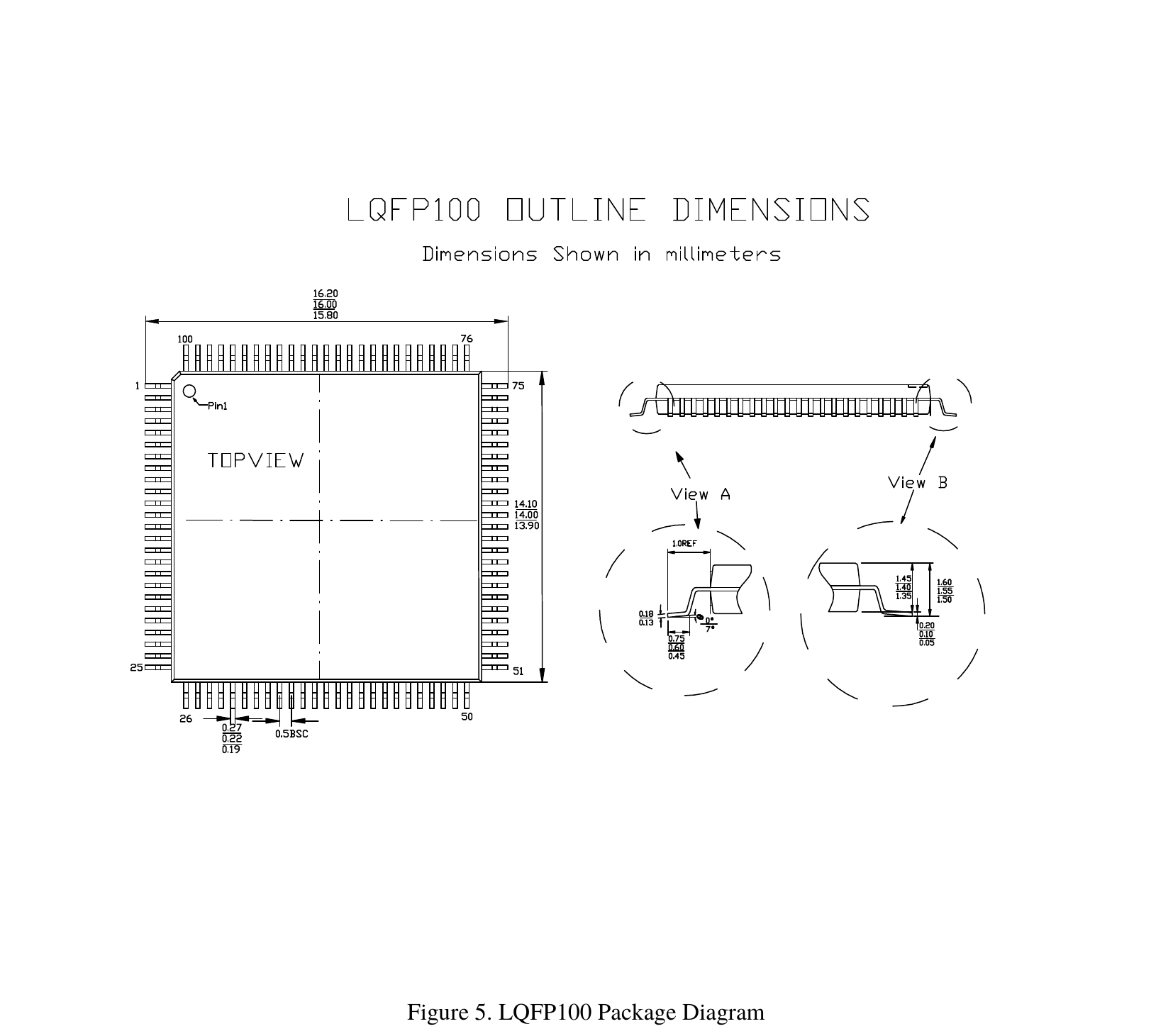
LQFP-100 plastic(14mm×14mm)
RoHS compliant
Applications
High Definition Video Capture Card
Security and Protection monitoring
Medical Image
Live Video Streaming
Function Block Diagram
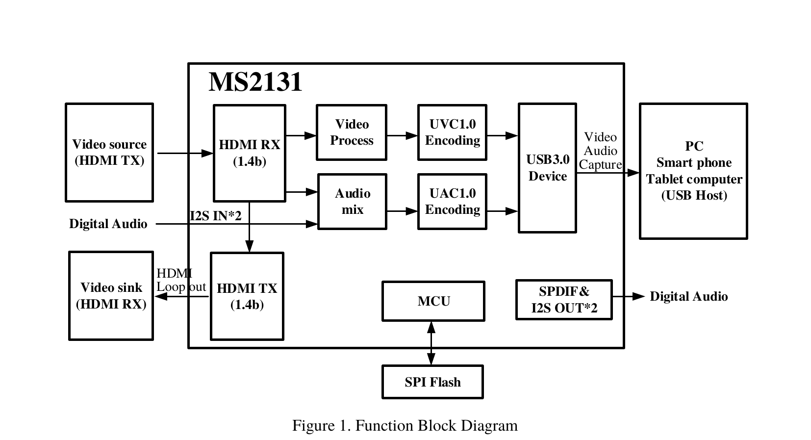
Function Description
GPIO
MS2131 has eight programmable GPIOs, which can be customized by software.
Audio Mixing Function
MS2131 supports 2 channels digital audio (I2S) input, HDMI RX audio processing, 2 channels digital audio (I2S) output, one SPDIF audio output, which can realize various mixing processing through software configuration to meet the application of different scenarios.
The audio mixing function application block diagram is shown in the figure below. For specific applications, please refer to the SDK User Guide.
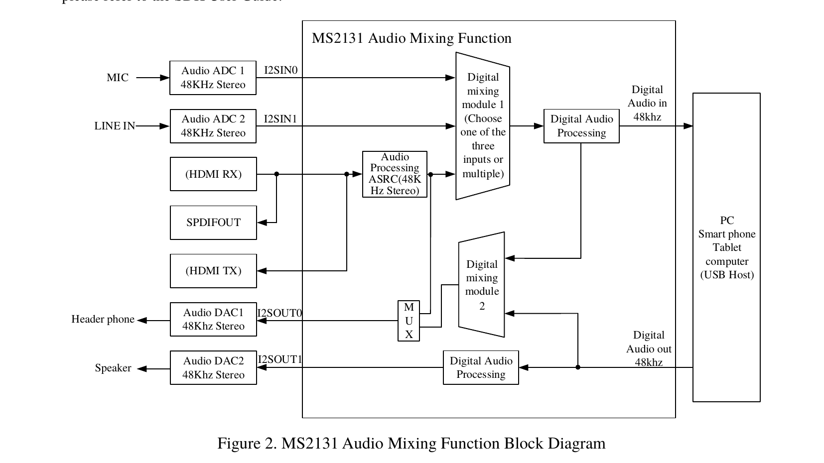
HDMI Loop Out Function
MS2131 supports USB to collect HDMI input audio and video data sources, and also supports HDMI video signal loop-out function. Supports HDCP & HPD processing, and EDID customization.
Item |
Description |
|---|---|
Display Product Name |
HDMI TO USB |
Best resolution 1 |
1080P@60Hz, 148.5MHz |
Video support resolution list |
640×480@60Hz |
Color space support |
RGB, YUV444, YUV422, YUV420 |
Deep color support |
30bits, 36bits |
Audio format support |
Format: L-PCM |
USB Video Output
MS2131 supports USB3.0 & USB2.0 mode video capture, and USB video conforms to UVC1.0 specification, supports YUV422 and MJPEG format video output and the default maximum output resolution 1920×1080@60Hz.
The MS2131 USB default output resolution list is as follows. The output resolution can be customized by the user by modifying the software configuration (support up to 4K@15Hz).
USB 3.0 Mode:
YUV422: |
MJPEG: |
|---|---|
1920×1080@60Hz/50Hz/30Hz/20Hz/10Hz |
1920×1080@60Hz/50Hz/30Hz/20Hz/10Hz |
1600×1200@60Hz/50Hz/30Hz/20Hz/10Hz |
1600×1200@60Hz/50Hz/30Hz/20Hz/10Hz |
1360×768@60Hz/50Hz/30Hz/20Hz/10Hz |
1360×768@60Hz/50Hz/30Hz/20Hz/10Hz |
1280×1024@60Hz/50Hz/30Hz/20Hz/10Hz |
1280×1024@60Hz/50Hz/30Hz/20Hz/10Hz |
1280×960@/60Hz/50Hz/30Hz/20Hz/10Hz |
1280×960@/60Hz/50Hz/30Hz/20Hz/10Hz |
1280×720@60Hz/50Hz/30Hz/20Hz/10Hz |
1280×720@60Hz/50Hz/30Hz/20Hz/10Hz |
1024×768@60Hz/50Hz/30Hz/20Hz/10Hz |
1024×768@60Hz/50Hz/30Hz/20Hz/10Hz |
800×600@60Hz/50Hz/30Hz/20Hz/10Hz |
800×600@60Hz/50Hz/30Hz/20Hz/10Hz |
720×576@60Hz/50Hz/30Hz/20Hz/10Hz |
720×576@60Hz/50Hz/30Hz/20Hz/10Hz |
720×480@60Hz/50Hz/30Hz/20Hz/10Hz |
720×480@60Hz/50Hz/30Hz/20Hz/10Hz |
640×480@60Hz/50Hz/30Hz/20Hz/10Hz |
640×480@60Hz/50Hz/30Hz/20Hz/10Hz |
USB 2.0 Mode:
YUV422: |
MJPEG: |
|---|---|
1920×1080@10Hz/5Hz |
1920×1080@50Hz/30Hz/25Hz/20Hz/10Hz |
1600×1200@10Hz/5Hz |
1600×1200@60Hz/50Hz/30Hz/20Hz/10Hz |
1360×768@15Hz/8Hz |
1360×768@60Hz/50Hz/30Hz/20Hz/10Hz |
1280×1024@15Hz/8Hz |
1280×1024@60Hz/50Hz/30Hz/20Hz/10Hz |
1280×960@15Hz/8Hz |
1280×960@/60Hz/50Hz/30Hz/20Hz/10Hz |
1280×720@20Hz/10Hz |
1280×720@60Hz/50Hz/30Hz/20Hz/10Hz |
1024×768@20Hz/10Hz |
1024×768@60Hz/50Hz/30Hz/20Hz/10Hz |
800×600@30Hz/20Hz/10Hz |
800×600@60Hz/50Hz/30Hz/20Hz/10Hz |
720×576@50Hz/25Hz/20Hz/10Hz |
720×576@60Hz/50Hz/30Hz/20Hz/10Hz |
720×480@60Hz/30Hz/20Hz/10Hz |
720×480@60Hz/50Hz/30Hz/20Hz/10Hz |
640×480@60Hz/30Hz/20Hz/10Hz |
640×480@60Hz/50Hz/30Hz/20Hz/10Hz |
USB Audio Output
MS2131 USB audio conforms to UAC1.0 specification, and the default output is 48KHz stereo. The audio output of other resolutions can be realized through software configuration.
PIN Map
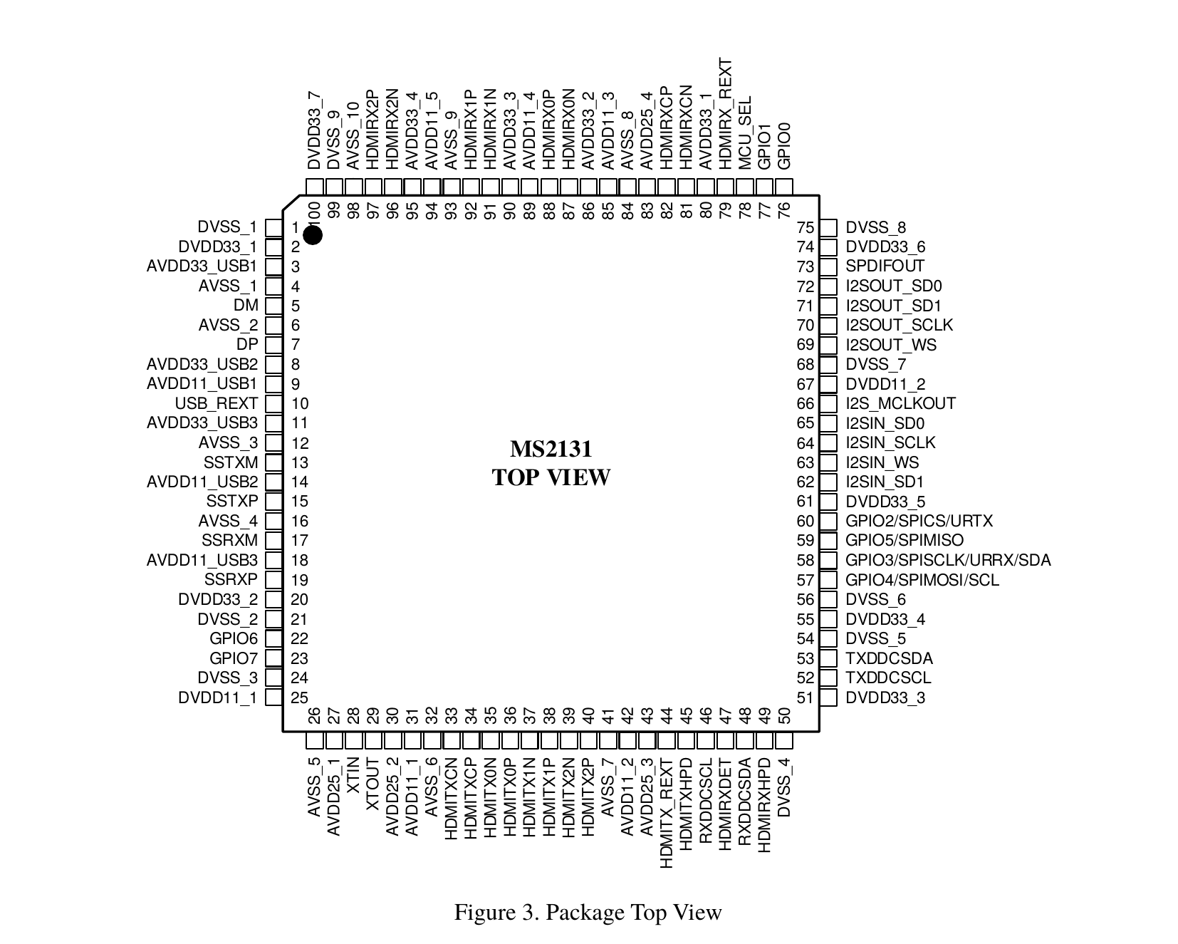
PIN Description
Pin Name |
Pin # |
Type |
Description |
|---|---|---|---|
GPIO |
|||
GPIO0 |
76 |
DIO |
General purpose digital IO |
GPIO1 |
77 |
DIO |
General purpose digital IO |
GPIO2/SPICS/URTX |
60 |
DIO |
General purpose digital IO, multiplexed with SPI Master interface CS pin and UART TX pin. If SPI interface flash is connected to the periphery, the chip will be automatically configured as SPICS function after power on |
GPIO3/SPISCLK/URRX/SDA |
58 |
DIO |
General purpose digital IO, multiplexed with SPI Master interface SCLK pin, UART RX pin and I2C Master SDA pin. If SPI interface flash is connected to the periphery, the chip will be automatically configured as SPISCLK function after power on |
GPIO4/SPIMOSI/SCL |
57 |
DIO |
General purpose digital IO, multiplexed with SPI Master interface MOSI pin and I2C Master SCL pin. If SPI interface flash is connected to the periphery, the chip will be automatically configured as SPIMOSI function after power on |
GPIO5/SPIMISO |
59 |
DIO |
General purpose digital IO, multiplexed with SPI Master interface MISO pin. If SPI interface flash is connected to the periphery, the chip will be automatically configured as SPIMISO function after power on |
GPIO6 |
22 |
DIO |
General purpose digital IO |
GPIO7 |
23 |
DIO |
General purpose digital IO |
USB |
|||
DP |
7 |
DIO |
USB 2.0 differential signal D+ |
DM |
5 |
DIO |
USB 2.0 differential signal D- |
USB_REXT |
10 |
AO |
Connect 200 resister to ground |
SSTXP |
15 |
DO |
USB 3.0 differential signal SSTX+ |
SSTXM |
13 |
DO |
USB 3.0 differential signal SSTX- |
SSRXP |
19 |
DI |
USB 3.0 differential signal SSRX+ |
SSRXM |
17 |
DI |
USB 3.0 differential signal SSRX- |
HDMI RX |
|||
HDMIRXCN |
81 |
DI |
HDMI RX Differential Clock Input Negative |
HDMIRXCP |
82 |
DI |
HDMI RX Differential Clock Input Positive |
HDMIRX0N |
87 |
DI |
HDMI RX Differential Data0 Input Negative |
HDMIRX0P |
88 |
DI |
HDMI RX Differential Data0 Input Positive |
HDMIRX1N |
91 |
DI |
HDMI RX Differential Data1 Input Negative |
HDMIRX1P |
92 |
DI |
HDMI RX Differential Data1 Input Positive |
HDMIRX2N |
96 |
DI |
HDMI RX Differential Data2 Input Negative |
HDMIRX2P |
97 |
DI |
HDMI RX Differential Data2 Input Positive |
HDMIRX_REXT |
79 |
AO |
Connect 1.6K resister to ground |
HDMIRXHPD |
49 |
DO |
HDMI RX HPD signal output |
HDMIRXDET |
47 |
DI |
HDMI RX 5V detection signal input |
RXDDCSDA |
48 |
DIO |
HDMI RX DDC SDA |
RXDDCSCL |
46 |
DI |
HDMI RX DDC SCL |
HDMI TX |
|||
HDMITXCN |
33 |
DO |
HDMI TX Differential Clock Input Negative |
HDMITXCP |
34 |
DO |
HDMI TX Differential Clock Input Positive |
HDMITX0N |
35 |
DO |
HDMI TX Differential Data0 Input Negative |
HDMITX0P |
36 |
DO |
HDMI TX Differential Data0 Input Positive |
HDMITX1N |
37 |
DO |
HDMI TX Differential Data1 Input Negative |
HDMITX1P |
38 |
DO |
HDMI TX Differential Data1 Input Positive |
HDMITX2N |
39 |
DO |
HDMI TX Differential Data2 Input Negative |
HDMITX2P |
40 |
DO |
HDMI TX Differential Data2 Input Positive |
HDMITX_REXT |
44 |
AO |
Connect 1.6K resister to ground |
HDMITXHPD |
45 |
DI |
HDMI TX hot plug signal output |
TXDDCSDA |
53 |
DIO |
HDMI TX DDC SDA |
TXDDCSCL |
52 |
DO |
HDMI TX DDC SCL |
Digital Audio |
|||
I2SIN_WS |
63 |
DIO |
I2SIN_WS signal is output in master mode by default and can be configured by software to work in slave mode. |
I2SIN_SCLK |
64 |
DIO |
I2SIN_SCLK signal is output in master mode by default and can be configured by software to work in slave mode. |
I2SIN_SD0 |
65 |
DI |
I2S input SD0 signal |
I2SIN_SD1 |
62 |
DI |
I2S input SD1 signal |
I2S_MCLKOUT |
66 |
DO |
12.288MHz clock output |
I2SOUT_WS |
69 |
DIO |
I2SOUT_WS signal is output in master mode by default and can be configured by software to work in slave mode. |
I2SOUT_SCLK |
70 |
DIO |
I2SOUT_SCLK signal is output in master mode by default and can be configured by software to work in slave mode. |
I2SOUT_SD0 |
72 |
DO |
I2S output SD0 signal |
I2SOUT_SD1 |
71 |
DO |
I2S output SD1 signal |
SPDIFOUT |
73 |
DO |
SPDIF format audio output |
Test PIN |
|||
MCU_SEL |
78 |
DI |
Test PIN, floating by default |
Crystal |
|||
XTIN |
28 |
AI |
24MHz passive crystal oscillator input |
XTOUT |
29 |
AO |
24MHz passive crystal oscillator output |
System Power & Ground |
|||
AVDD33_USB1~3 |
3,8,11 |
P |
Analog Power (USB 3.3V) |
AVDD33_1~4 |
80,86,90,95 |
P |
Analog Power (3.3V) |
DVDD33_1~7 |
2,20,51,55,61,74,100 |
P |
Digital IO Power (3.3V) |
AVDD25_1~4 |
27,30,43,83 |
P |
Analog Power (2.5V) |
AVDD11_USB1~3 |
9,14,18 |
P |
Analog Power (USB 1.1V) |
DVDD11_1~2 |
25,67 |
P |
Digital Power (1.1V) |
AVDD11_1~5 |
31,42,85,89,94 |
P |
Analog Power (1.1V) |
AVSS_1~10 |
4,6,12,16,26,32,41,84,93,98 |
G |
Ground (Analog) |
DVSS_1~9 |
1,21,24,50,54,56,68,75,99 |
G |
Ground (Digital) |
Abbreviation |
Description |
|---|---|
AI |
Analog Input |
AO |
Analog Output |
DI |
Digital Input |
DO |
Digital Output |
DIO |
Digital Bi-direction |
P |
Power |
G |
Ground |
Electrical Characteristics
Absolute Maximum Ratings
Parameter |
Symbol |
Value |
Unit |
|---|---|---|---|
Maximum Operating Voltage(AVDD33 / DVDD33 / DVDDIO) |
VDD33 |
3.63 |
V |
Maximum Operating Voltage(AVDD25) |
VDD25 |
2.75 |
V |
Maximum Operating Voltage(AVDD11 and DVDD11) |
VDD11 |
1.21 |
V |
Voltage On Any Pin With Respect to Ground |
VI |
-0.5 to DVDD33+0.5 |
V |
Ambient Operating Temperature |
TA |
0 to 70 |
°C |
Storage Temperature |
Tsto |
-65 to +150 |
°C |
Allowable Junction Temperature |
Tjmax |
125 |
°C |
Note1: Stresses beyond those listed under “Absolute Maximum Ratings” may cause permanent damage to the device. This is a stress rating only and functional operation of the device at these or other conditions beyond those indicated in the operational sections of this specification is not implied. Exposure to absolute maximum rating conditions for extended periods may affect device reliability.
Parameter |
Symbol |
Value |
Unit |
|---|---|---|---|
Junction-to-ambient Thermal Resistance (JEDEC 4-layer test board) |
RθJA |
30 |
°C/W |
Junction-to-board Thermal Resistance |
RθJB |
8 |
°C/W |
Junction-to-case Thermal Resistance |
RθJC |
12 |
°C/W |
DC Characteristics
Parameter |
MIN |
Typical |
MAX |
Unit |
Condition |
|---|---|---|---|---|---|
VDD33 |
3.135 |
3.3 |
3.465 |
V |
GND = 0V, TA = +25°C unless otherwise noted |
VDD25 |
2.375 |
2.5 |
2.625 |
V |
GND = 0V, TA = +25°C unless otherwise noted |
VDD11 |
1.045 |
1.1 |
1.155 |
V |
GND = 0V, TA = +25°C unless otherwise noted |
Input Low Voltage |
-0.3 |
0.8 |
V |
||
Input High Voltage |
2.0 |
3.6 |
V |
Note1:VDD33 includes AVDD33_USB, DVDD33, AVDD33. VDD11 includes AVDD11_USB, DVDD11, AVDD11.
Power Consumption in Different Modes
Condition: GND = 0V, TA = +25°C.
Parameter |
UVC ON, USB Input 1080P@60Hz, HDMI loop out 4K@30Hz |
UVC OFF, HDMI no source |
USB Suspend |
Unit |
|---|---|---|---|---|
VDD33 |
0.48 |
0.066 |
0.033 |
W |
VDD25 |
0.12 |
0.012 |
0.004 |
W |
VDD11 |
0.22 |
0.053 |
0.012 |
W |
USB Video input fixed at 1920×1080@60Hz, YUV mode; HDMI loop out, the typical value of current in different resolution modes.
Condition: GND = 0V, TA = +25°C.
Parameter |
4K@30Hz |
1080P@60Hz |
720P@60Hz |
Unit |
|---|---|---|---|---|
AVDD33 |
110 |
98 |
85 |
mA |
DVDD33 |
35 |
35 |
26 |
mA |
AVDD25 |
50 |
46 |
45 |
mA |
AVDD11 |
115 |
87 |
75 |
mA |
DVDD11 |
85 |
75 |
66 |
mA |
Typical Application Circuit
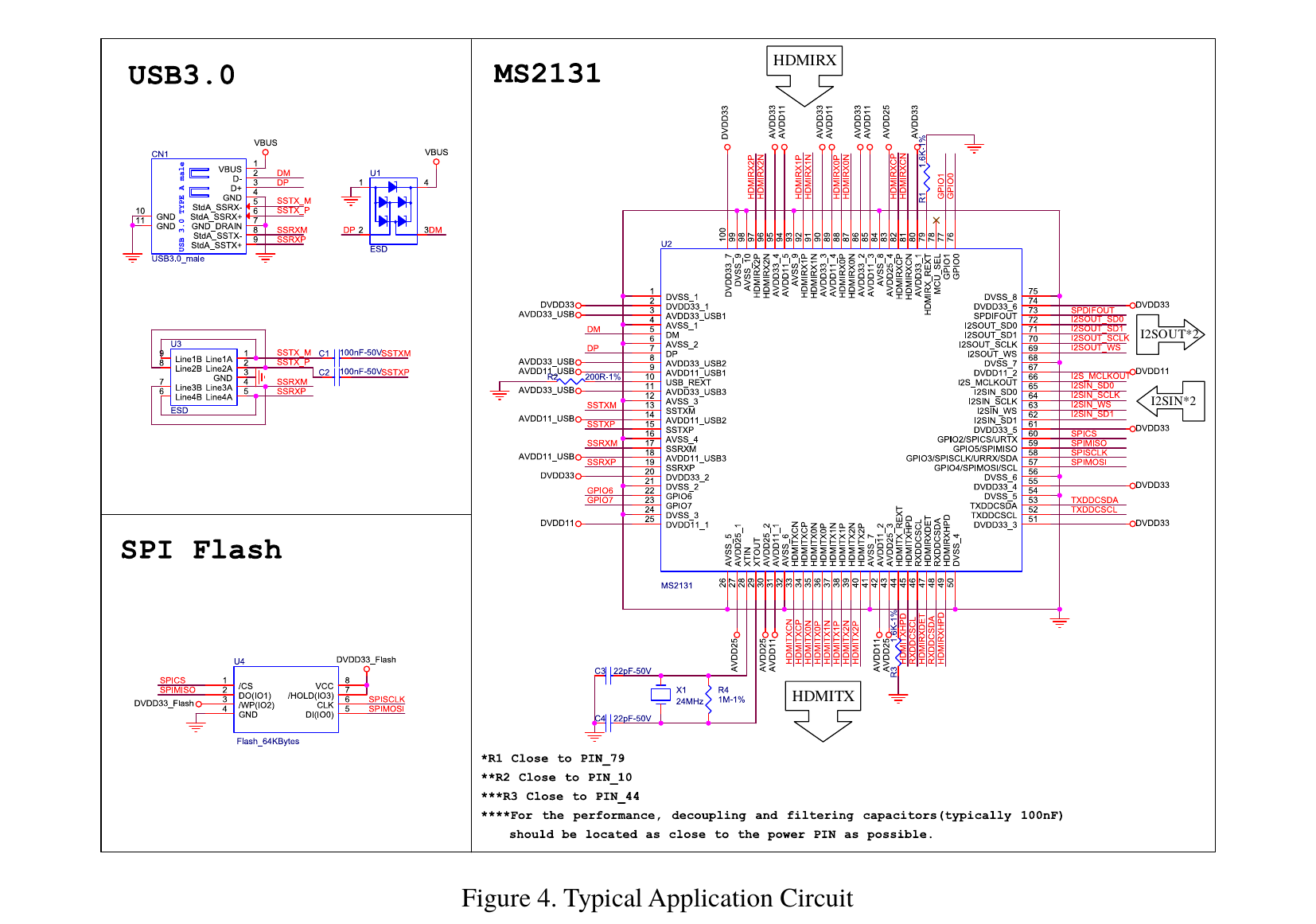
Package Outline
Top Mark
Packing Information
Packing Information
Packing carton dimension (Unit: mm) |
|
|---|---|
Inner Carton |
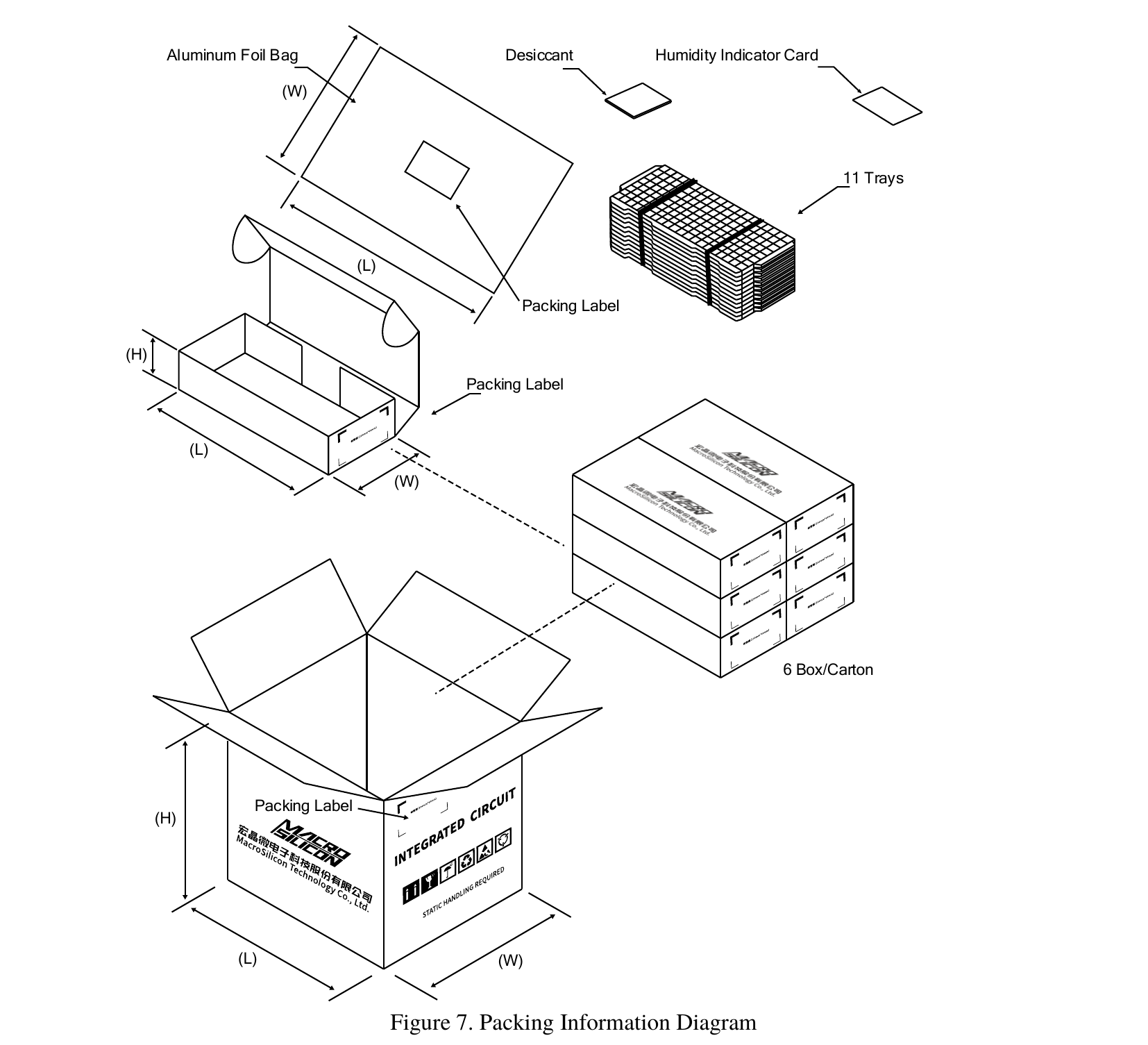
370(L)*155(W)*85(H) |
Outer Carton |
390(L)*330(W)*280(H) |
Package Outline |
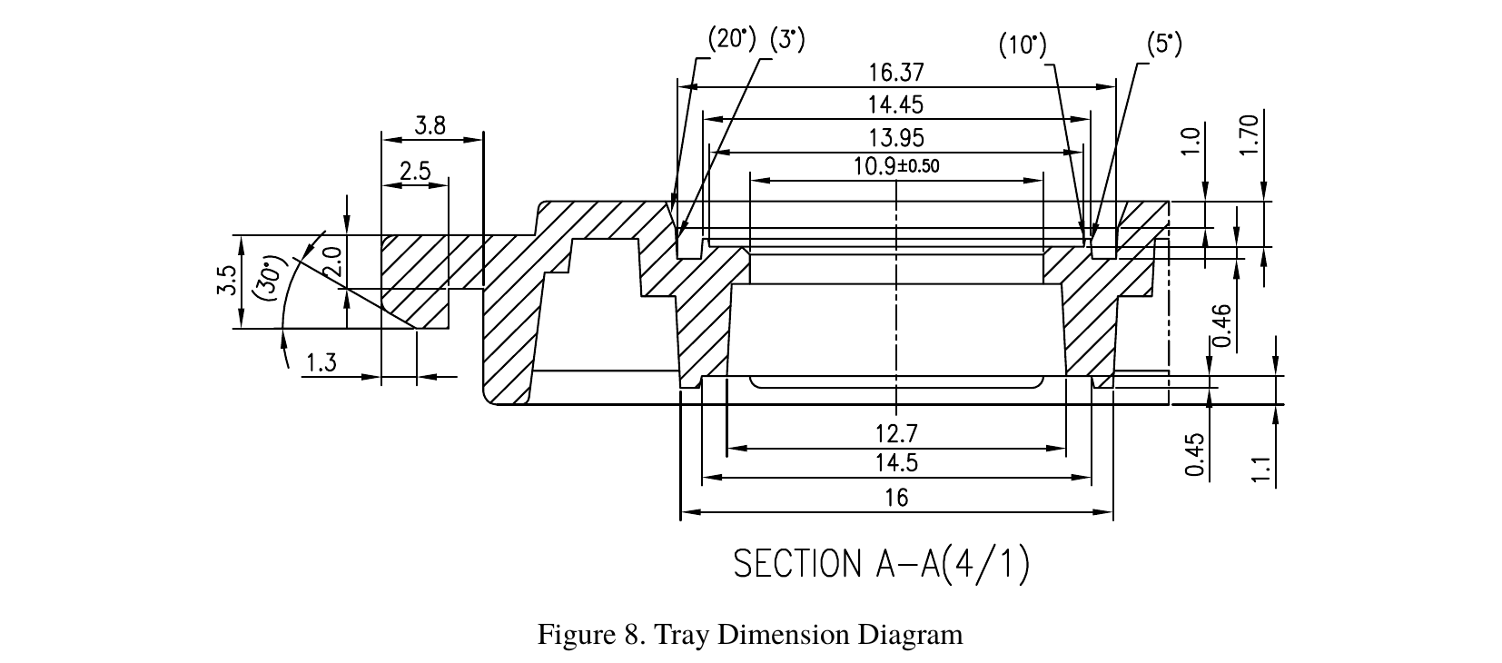
Quantity per TRAY (Unit:PCS) |
Quantity per inner carton (Unit:PCS) |
Quantity per outer carton (Unit:PCS) |
Inner Carton: Outer Carton |
|---|---|---|---|---|
LQFP100(14X14) |
90 |
900 |
5400 |
6:1 |
Carrier Tray Dimension
Reflow Specifications
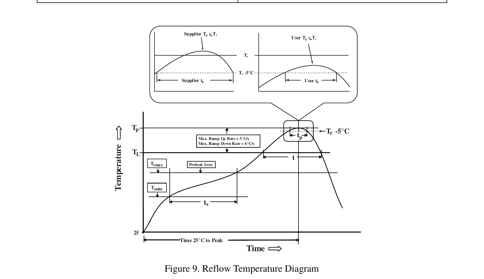
Reflow Profile |
Pb-Free Assembly |
|---|---|
Preheating time (Tsmin to Tsmax) |
60~120 seconds (150~200°C) |
Liquidous Temperature (TL) |
217°C |
Peak Temperature (TP) |
260°C (+5/-0°C) |
Ramp-up Rate (TL to TP) |
≤ 3.0°C/seconds |
Time Maintained above TL |
60~150 seconds |
Time Within 5°C of Peak Temperature (above 255°C) |
30~40 seconds |
Ramp-up Rate (TP to TL) |
≤ 6.0°C/seconds |
Time 25°C to Peak Temperature |
≤ 8 minutes |
PCB Design Guidelines
Power and Ground
Power trace width should correspond to the current flowing through it. Refer to the current values in the Electrical Characteristics section. Recommended minimum trace widths:
Maximum Current (mA) |
Recommended Trace Width (mil) |
|---|---|
50 |
≥12 |
100 |
≥16 |
200 |
≥20 |
400 |
≥30 |
Note: Above values are based on 1oz copper.
Decoupling capacitors must be placed close to the power pins of the chip
Power must flow through capacitors before entering the chip pins
Decoupling capacitor ground should be connected to power ground via nearby vias
Clock
Place crystal oscillator close to the chip
Keep routing as short as possible
Ground pour around the crystal required
No traces should be routed on the layer below the crystal to ensure complete ground plane
USB Signal Lines
USB differential pairs (SSTXP/M, SSRXP/M, and DP/M):
Impedance matching required: 90±10% Ohms
Differential pair routing should be as short as possible (no more than one via pair)
Pair-to-pair skew: within 5mil
Total length recommended: not exceeding 2000mil
Ground pour required around differential pairs
Maintain 3W rule (keep other signals at 3x trace width distance)
No traces on layer below to ensure complete ground plane
HD Signal Lines
HD differential pairs:
Impedance matching required: 100±10% Ohms
Keep differential pair routing short (no more than two via pairs)
Recommended intra-pair skew: within 5mil
Recommended inter-group skew: within 15mil
Ground pour required around differential pairs
Maintain 3W rule (keep other signals at 3x trace width distance)
No traces on layer below to ensure complete ground plane
Place ESD devices, common-mode inductors, and series resistors close to HD connectors
Component placement order: HD Connector → ESD Device → Common-mode Inductor → Series Resistor
Reference Design
Schematic
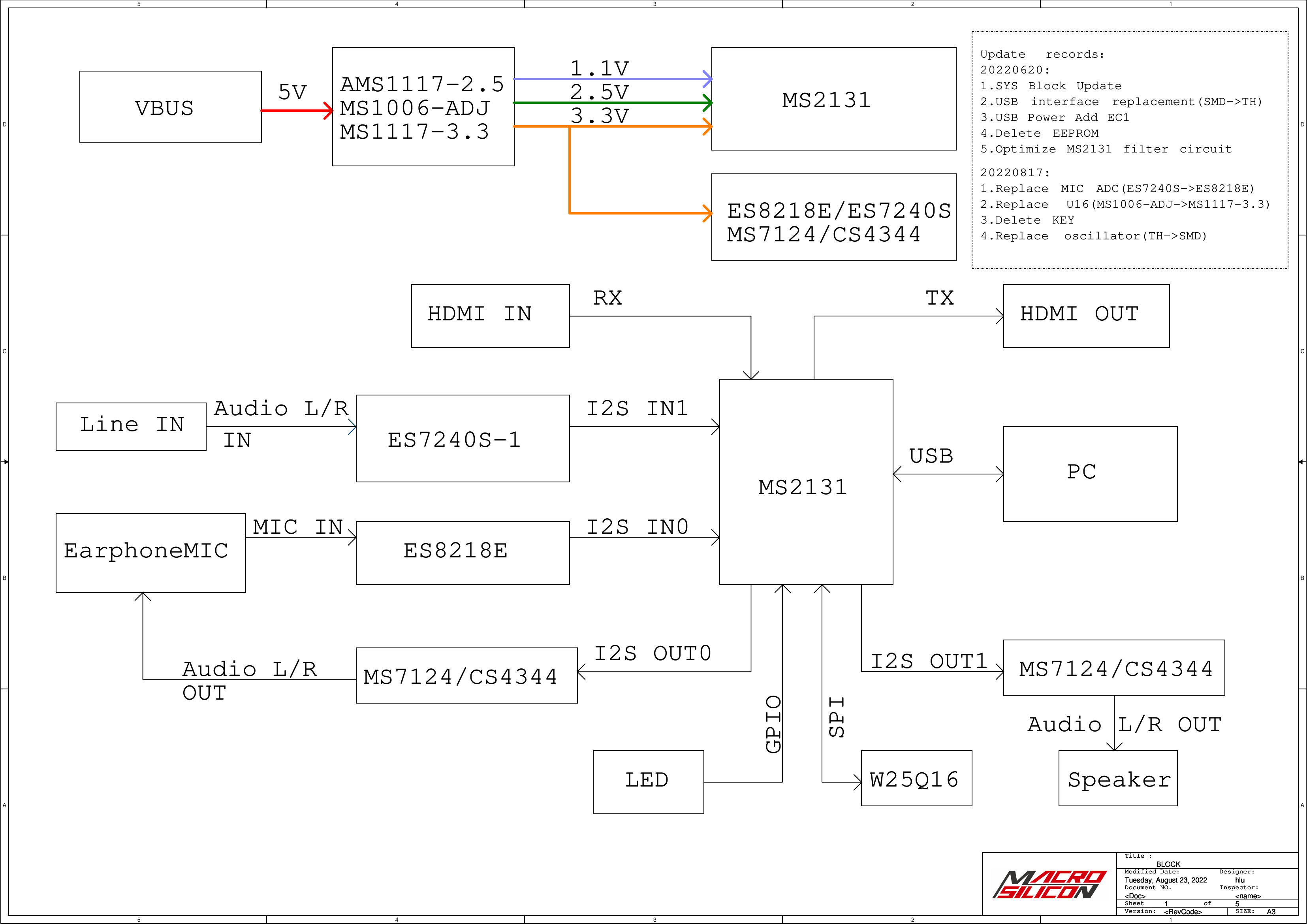
Block Diagram
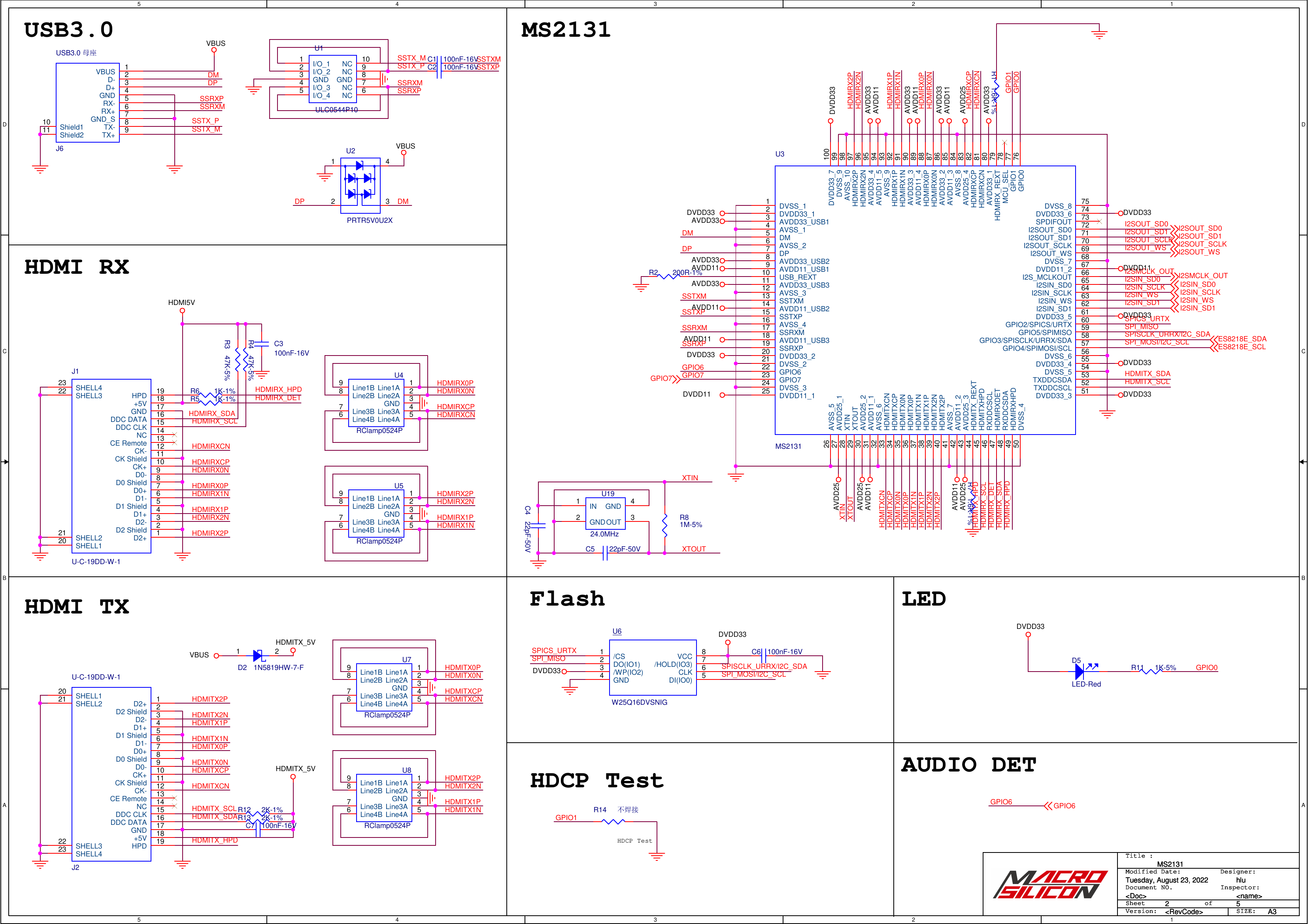
MS2131 Main Chip
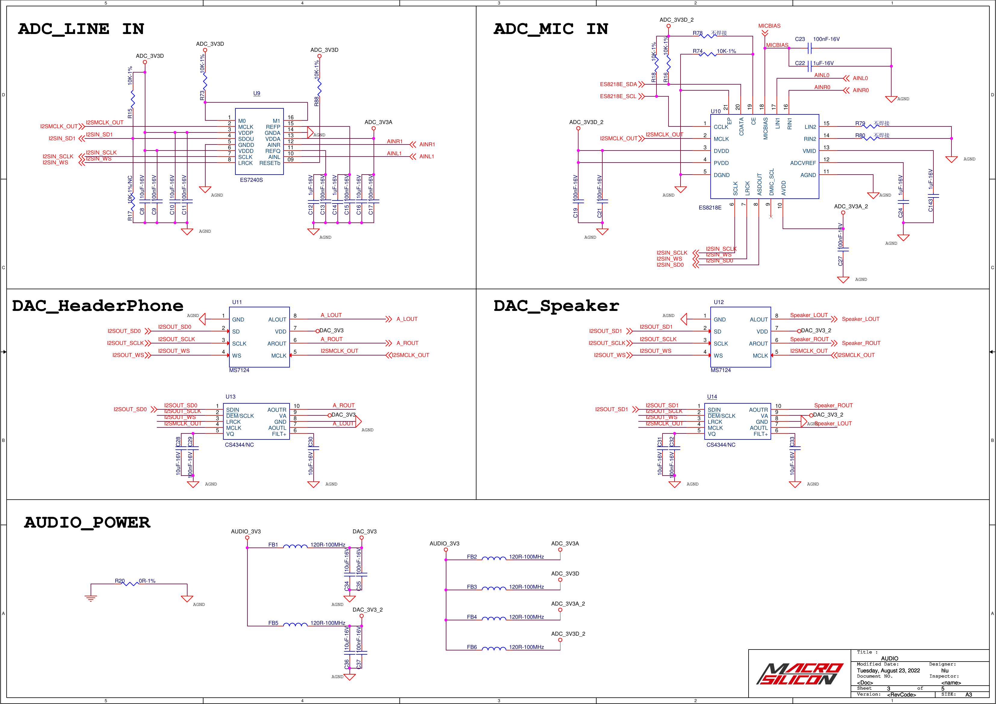
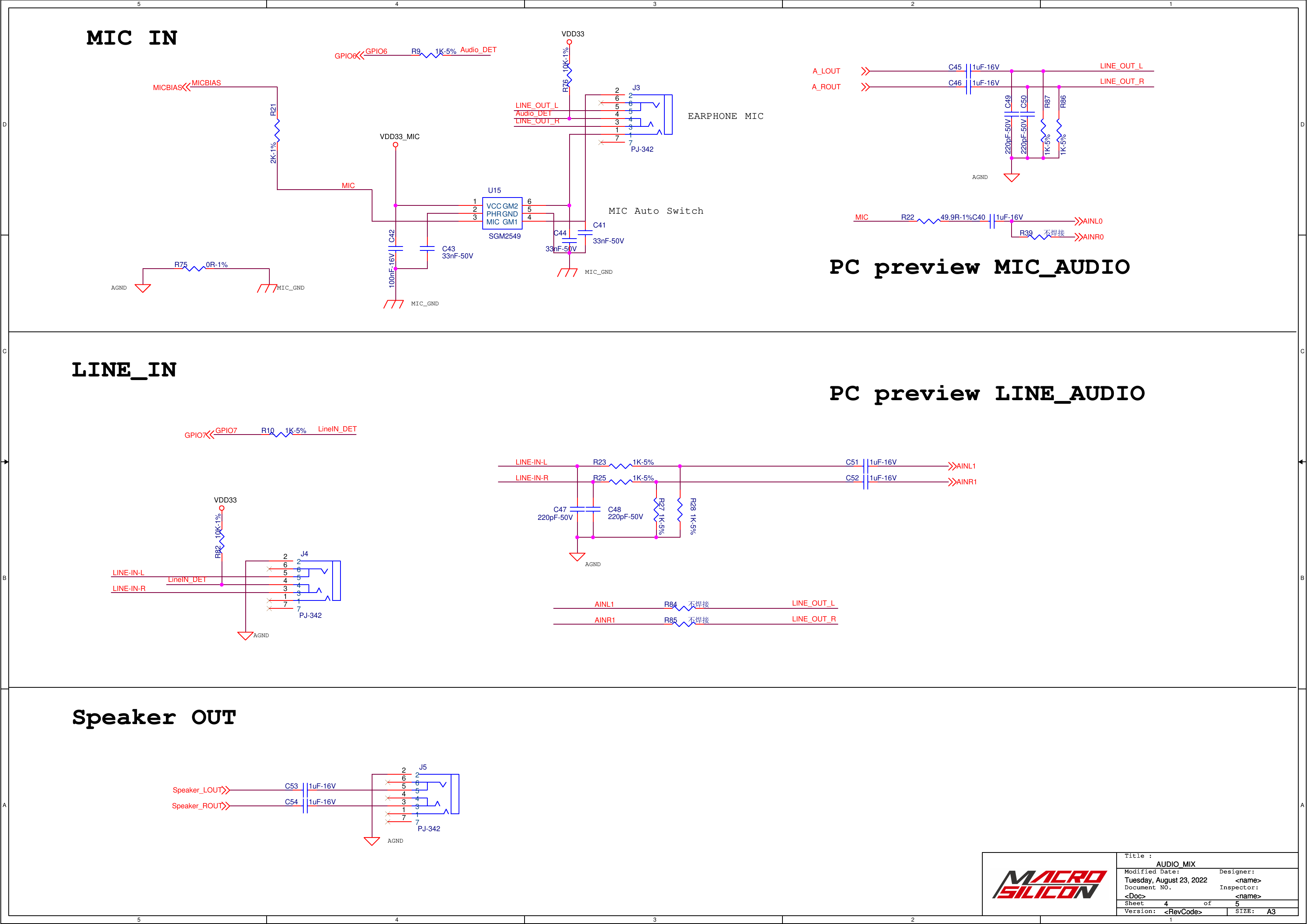
Audio Interface
Audio Mixing
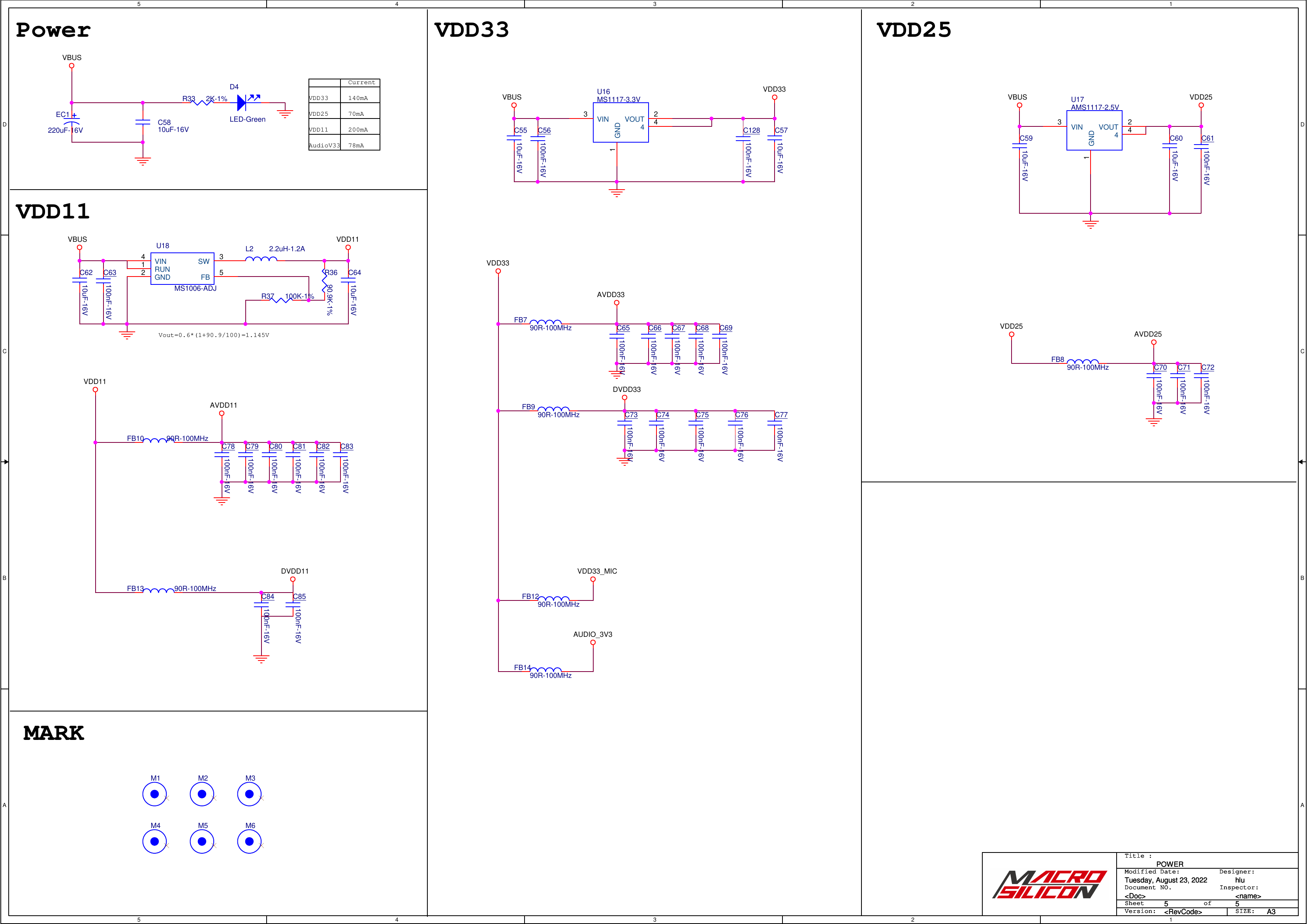
Power Distribution
Bill of Materials (BOM)
Item # |
Qty |
Reference Designators |
Part Number |
Footprint |
Description |
|---|---|---|---|---|---|
1 |
44 |
C1,C2,C3,C6,C7,C9,C11,C13,C15,C17,C19,C21,C23,C27,C29,C32,C35,C37,C42,C56,C61,C63,C65,C66,C67,C68,C69,C70,C71,C72,C73,C74,C75,C76,C77,C78,C79,C80,C81,C82,C83,C84,C85,C128 |
100nF-16V |
C0402 |
Decoupling capacitors |
2 |
2 |
C4,C5 |
22pF-50V |
C0402 |
Crystal load capacitors |
3 |
16 |
C8,C10,C16,C28,C30,C31,C33,C34,C36,C55,C57,C58,C59,C60,C62,C64 |
10uF-16V |
C0603 |
Bulk decoupling capacitors |
4 |
12 |
C12,C14,C22,C24,C40,C45,C46,C51,C52,C53,C54,C143 |
1uF-16V |
C0402 |
Low-ESR capacitors |
5 |
3 |
C41,C43,C44 |
33nF-50V |
C0603 |
Audio coupling capacitors |
6 |
4 |
C47,C48,C49,C50 |
220pF-50V |
C0402 |
High-frequency filtering |
7 |
1 |
D2 |
1N5819HW-7-F |
SOD-123 |
Schottky diode |
8 |
1 |
D4 |
LED-Green |
LED0603 |
Status indicator (green) |
9 |
1 |
D5 |
LED-Red |
LED0603 |
Status indicator (red) |
10 |
1 |
EC1 |
220uF-16V |
CAP-6.3X6.6-SMD |
Electrolytic capacitor |
11 |
6 |
FB1,FB2,FB3,FB4,FB5,FB6 |
120R-100MHz |
L0603 |
Ferrite beads |
12 |
7 |
FB7,FB8,FB9,FB10,FB12,FB13,FB14 |
90R-100MHz |
L0603 |
Ferrite beads |
13 |
2 |
J1,J2 |
U-C-19DD-W-1 |
HDMI-19P-TH |
HDMI connectors (input/output) |
14 |
3 |
J3,J4,J5 |
PJ-342 |
PJ-342 |
3.5mm audio jacks |
15 |
1 |
J6 |
USB3.0 Female |
USB-AF-W-3.0 |
USB 3.0 type-A connector |
16 |
1 |
L2 |
2.2uH-1.2A |
LP-2.0X1.6 |
Inductor |
17 |
6 |
M1,M2,M3,M4,M5,M6 |
MARK |
MARK |
Board markings/test points |
18 |
2 |
R1,R7 |
1.6K-1% |
R0402 |
Impedance terminators (HD) |
19 |
1 |
R2 |
200R-1% |
R0402 |
USB terminator |
20 |
2 |
R3,R4 |
47K-5% |
R0402 |
Pull-up resistors |
21 |
2 |
R5,R6 |
1K-1% |
R0402 |
Current limit resistors |
22 |
1 |
R8 |
1M-5% |
R0402 |
High-impedance resistor |
23 |
9 |
R9,R10,R11,R23,R25,R27,R28,R86,R87 |
1K-5% |
R0402 |
Pull-up/pull-down resistors |
24 |
4 |
R12,R13,R21,R33 |
2K-1% |
R0402 |
Signal resistors |
25 |
7 |
R14,R39,R78,R79,R80,R84,R85 |
NC |
R0402 |
No-connect positions |
26 |
8 |
R15,R16,R18,R73,R74,R76,R82,R88 |
10K-1% |
R0402 |
Pull-up resistors |
27 |
1 |
R17 |
10K-1%/NC |
R0402 |
Configurable resistor |
28 |
2 |
R20,R75 |
0R-1% |
R0402 |
Jumper resistors |
29 |
1 |
R22 |
49.9R-1% |
R0402 |
Impedance matching |
30 |
1 |
R36 |
90.9K-1% |
R0402 |
Precision resistor |
31 |
1 |
R37 |
100K-1% |
R0402 |
Precision resistor |
32 |
1 |
U1 |
ULC0544P10 |
DFN2510-10 |
ESD protection (USB) |
33 |
1 |
U2 |
PRTR5V0U2X |
SOT143B |
ESD protection (HDMI) |
34 |
1 |
U3 |
MS2131 |
LQFP100-14X14X05P |
Main chip |
35 |
4 |
U4,U5,U7,U8 |
RClamp0524P |
SPL2510P8 |
ESD protection (HDMI) |
36 |
1 |
U6 |
W25Q16DVSNIG |
SOIC8-1.27-150MIL |
SPI Flash (16Mb) |
37 |
1 |
U9 |
ES7240S |
TSSOP16-0.65-6.0 |
I2S audio interface |
38 |
1 |
U10 |
ES8218E |
QFN20-3X3X04P |
Audio codec |
39 |
2 |
U11,U12 |
MS7124 |
SOIC8-1.27-150MIL |
Audio amplifier |
40 |
2 |
U13,U14 |
CS4344/NC |
TSSOP10-0.5-4.2 |
DAC (optional) |
41 |
1 |
U15 |
SGM2549 |
SOT-23-6 |
High-side switch |
42 |
1 |
U16 |
MS1117-3.3V |
SOT-223 |
LDO regulator (3.3V) |
43 |
1 |
U17 |
AMS1117-2.5V |
SOT-223 |
LDO regulator (2.5V) |
44 |
1 |
U18 |
MS1006-ADJ |
SOT-23-5 |
Adjustable regulator |
45 |
1 |
U19 |
24.0MHz |
XTAL-3225 |
System clock oscillator |
Component Placement
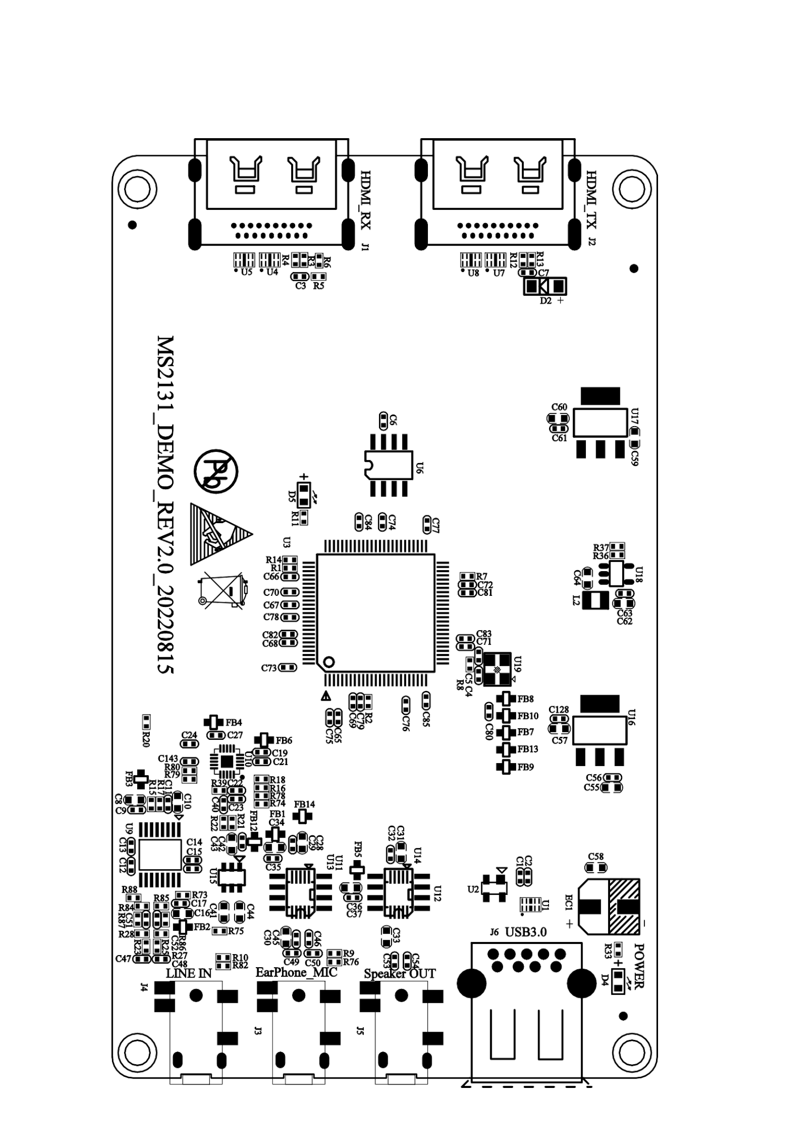
Top Placement
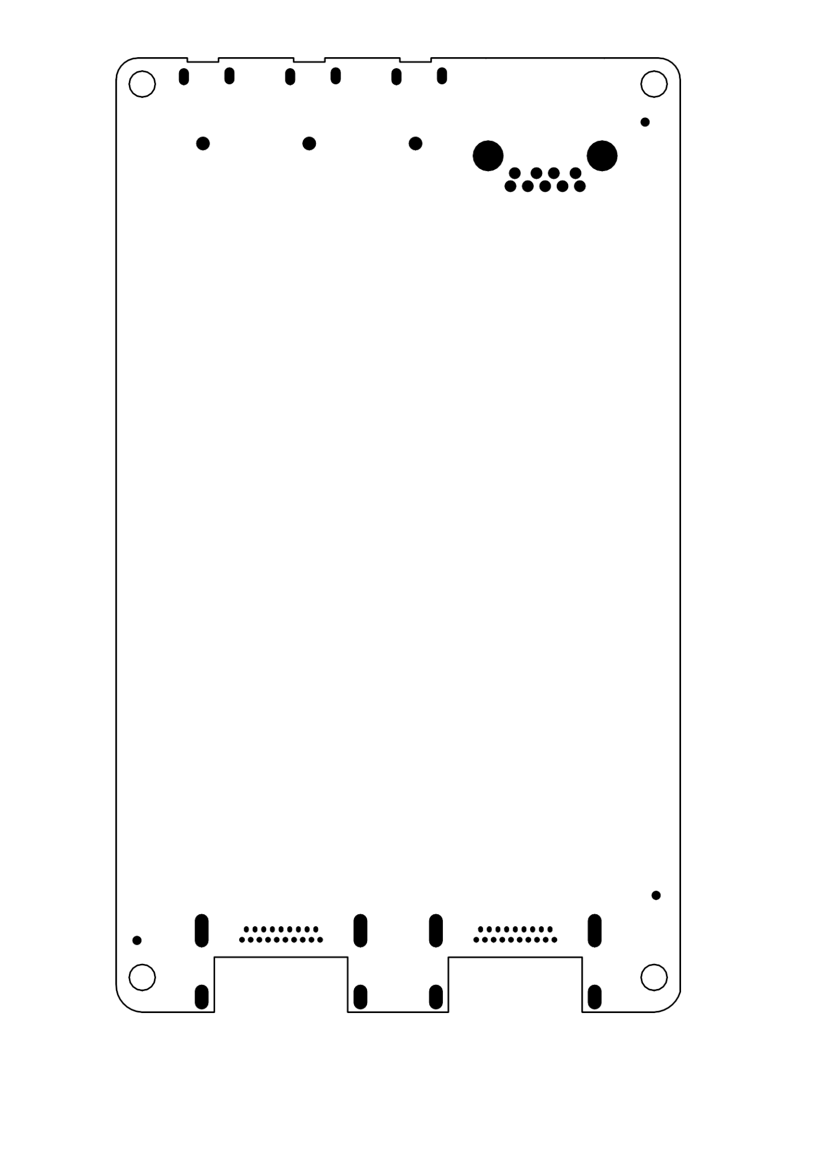
Bottom Placement
Key Features
USB Interface: USB 3.0 female connector for high-speed data transfer
HDMI I/O: One HDMI input and one HDMI output for video capture and passthrough
Audio I/O: 3.5mm connectors for microphone input and audio outputs (headphone/speaker)
Audio Mixing: On-board mixing of multiple audio sources via ES8218E codec
Power Supply: Multiple voltage regulators providing 3.3V, 2.5V, and 1.1V rails
ESD Protection: Multiple ESD protection devices for all external interfaces
Storage: 16Mb SPI flash for firmware storage
Connectors
Connector |
Type |
Function |
|---|---|---|
J1 |
HDMI-19P |
HDMI Input |
J2 |
HDMI-19P |
HDMI Output |
J3 |
3.5mm |
Microphone Input |
J4 |
3.5mm |
Headphone Output |
J5 |
3.5mm |
Speaker Output |
J6 |
USB 3.0-A |
USB 3.0 Data/Power |
Firmware Layout
MS2130 MS2131
ROM Address |
Flash Address |
Length |
User Data |
data type |
|---|---|---|---|---|
0x00F800 |
0x00F830 |
0x100 |
edid |
uint8 array[256] |
0x00F900 |
0x00F930 |
0x120 |
hdcpUserKey |
uint8 array[288] |
0x00FA20 |
0x00FA50 |
0x020 |
ultrasemi |
uchar array[32] |
0x00FA40 |
0x00FA70 |
0x020 |
ultrasemi_version |
uchar array[32] |
0x00FA60 |
0x00FA90 |
0x020 |
ultrasemi_magic |
uint8 array[32] |
0x00FA80 |
0x00FAB0 |
0x020 |
ManufacturerString |
user_string_t |
0x00FAA0 |
0x00FAD0 |
0x020 |
ProduceString |
user_string_t |
0x00FAC0 |
0x00FAF0 |
0x020 |
U2ProduceString |
user_string_t |
0x00FAE0 |
0x00FB10 |
0x020 |
AudioString |
user_string_t |
0x00FB00 |
0x00FB30 |
0x020 |
U2AudioString |
user_string_t |
0x00FB20 |
0x00FB50 |
0x020 |
SerialnumString |
user_string_t |
0x00FB40 |
0x00FB70 |
0x020 |
U2SerialnumString |
user_string_t |
0x00FB60 |
0x00FB90 |
0x020 |
BCSH |
user_bcsh_t |
0x00FB80 |
0x00FBB0 |
0x020 |
AudioRoute |
audio_route_t |
user_string_t
[Offset 0] length : uint8
2 ~ 31
[Offset 1:31] char array : uchar
user_bcsh_t
Index |
data type |
data name |
— |
|---|---|---|---|
0 |
UINT8 |
bcsh_en |
0x01: User BCSH data Enable |
1 |
INT8 |
b |
-127 ~ 128 |
2 |
UINT8 |
c |
0 ~ 255 |
3 |
UINT8 |
s |
0 ~ 255 |
3 |
INT8 |
h |
-127 ~ 128 |
audio_route_t
[Offset 0] sample_rate : UINT8
0 : AUDIO_SR_48000
1 : AUDIO_SR_96000
other : Not used
[Offset 1] i2s_in_mode : UINT8
0 : slave
1 : master
other : Not used
[Offset 2] mix3_mode : UINT8
1 : HDMI RX
2 : I2S1 IN
3 : I2S1 IN & HDMI RX
4 : I2S2
5 : I2S2 IN & HDMI RX
6 : I2S1 IN & I2S2 IN
7 : I2S1 IN & I2S2 IN & HDMI RX
other : Not used
[Offset 3] i2s1_mode : UINT8
9 : HDMI RX
10 : MIX3 & USB OUT
11 : MIX3
12 : USB OUT
other : Not used
[Offset 4] usb_out_mute : UINT8
0 : unmute
1 : mute
other : Not used
[Offset 5] lk621_en : UINT8
0x00 : none
0x01 : config lk621 @0x26
0x02 : config lk621 @0x20
0x03 : config lk621 both
other : Not used
HIDCMD
reserved 0x10~0x3F, 0xA0~0xFF
B0 |
B1 |
B2 |
B3 |
B4 |
B5 |
B6 |
B7 |
|
|---|---|---|---|---|---|---|---|---|
cmd name |
cmd code |
|||||||
SFR RD |
C5 |
ADDR |
||||||
SFR WR |
C6 |
ADDR |
DATA |
|||||
IDATA RD |
B5 |
00 |
ADDR |
|||||
IDATA WR |
B6 |
00 |
ADDR |
DATA |
||||
IDATA RD |
B5 |
ADDR_H |
ADDR_L |
|||||
IDATA WR |
B6 |
ADDR_H |
ADDR_L |
DATA |
||||
FLASH RD |
F7 |
01 |
00 |
PAGE_ADDR_H |
PAGE_ADDR_L |
LEN_H |
LEN_L |
00 |
FLASH RD |
F7 |
00 |
00 |
PAGE_ADDR_H |
PAGE_ADDR_L |
ADDR_H |
ADDR_L |
00 |
FLASH WR |
F8 |
01 |
00 |
00 |
00 |
PAGE_ADDR_H |
PAGE_ADDR_L |
00 |
FLASH WR |
F8 |
00 |
D0 |
D1 |
D2 |
D3 |
D4 |
D5 |
MS2130 MS2131 MS2109 color and contrast
MS2130 |
MS2130 BCSH |
MS2109 |
|
|---|---|---|---|
Brightness |
-11 |
0 |
? |
Contrast |
148 |
128 |
? |
Saturation |
180 |
128 |
? |
Hue |
0 |
0 |
? |